Unveiling the Lattice LCMXO2-2000HC-5TG144I: A Comprehensive Guide to its Architecture and Applications
The Lattice LCMXO2-2000HC-5TG144I represents a pivotal component in the realm of low-power, high-performance programmable logic. As a member of Lattice Semiconductor's renowned MachXO2™ family, this device is engineered to bridge the gap between traditional CPLDs and larger FPGAs, offering a unique blend of flexibility, integration, and cost-effectiveness. This article delves into the core architecture of this FPGA and explores its diverse application landscape.
Architectural Deep Dive
At the heart of the LCMXO2-2000HC lies a sophisticated yet power-optimized architecture. Its core consists of 2,160 Look-Up Tables (LUTs), which serve as the fundamental building blocks for implementing custom logic functions. This logic fabric is complemented by 92 Kbits of embedded block RAM (EBR), providing efficient on-chip memory for data buffering and storage, and 66 Kbits of distributed RAM, offering additional flexible memory resources.
A standout feature of the MachXO2 series is its high level of system integration. The device incorporates hardened IP blocks that eliminate the need for external components, thereby reducing board space and total system cost. These include:
Pre-engineered SPI controller: Simplifies flash memory interfacing and enables instant-on functionality.
Dual I2C controllers: Facilitates communication with a vast ecosystem of sensors and peripheral chips.
User Flash Memory (UFM): Offers 256 Kbits of non-volatile storage for critical data like device serial numbers, user preferences, or small boot code.
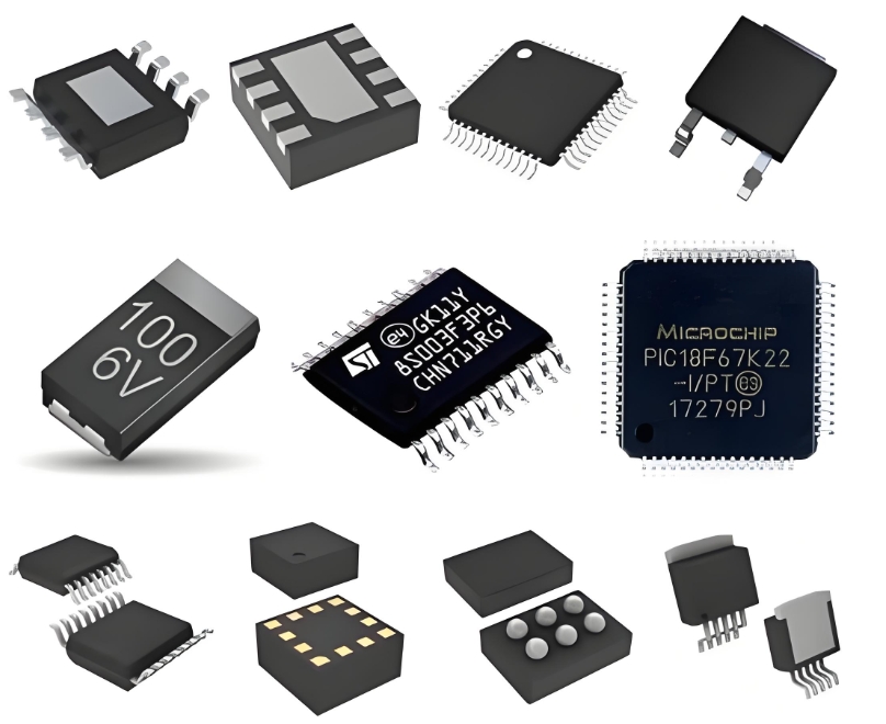
The "5TG144I" suffix provides critical package information: it is in a 5x5mm, 0.5mm pitch TQFP-144 package, making it suitable for space-constrained designs, and is specified for the Industrial temperature range (-40°C to 100°C).

Key Applications and Use Cases
The combination of low static power (as low as 19 µW), instant-on capability, and high integration makes the LCMXO2-2000HC-5TG144I exceptionally versatile. Its primary applications include:
1. System Management and Control: It is perfectly suited to act as a "system control hub" or a "universal glue logic" solution on complex PCBs. It can manage power sequencing, supervise microcontroller resets, interface with multiple sensors via I2C/SPI, and handle fan control, thereby offloading these tasks from a main CPU.
2. Sensor Aggregation and Data Bridging: In IoT and industrial sensing platforms, this FPGA can aggregate data from multiple analog and digital sensors, perform preliminary processing or filtering, and bridge the data to a host processor using protocols like SPI, I2C, or parallel interfaces.
3. Consumer Electronics: Its low power consumption is ideal for portable and battery-operated devices. It can manage interfaces, implement custom logic for touch controllers, or handle display bridging (e.g., LVDS to MIPI conversion).
4. Communications Infrastructure: It finds roles in network equipment for performing interface level translation (e.g., between different voltage levels), bus arbitration, and implementing custom serial protocols like 1-Wire or CAN.
5. Automotive and Industrial: Its industrial temperature rating allows it to thrive in harsh environments. It is used for motor control, in-vehicle infotainment (IVI) system interfacing, and industrial automation control logic.
The Lattice LCMXO2-2000HC-5TG144I is a highly integrated, ultra-low-power FPGA that excels in control-oriented applications. Its unique value proposition lies in its ability to replace multiple discrete logic components and ASSPs, simplifying board design, enhancing reliability, and reducing the overall bill of materials (BOM). For designers seeking a flexible, cost-effective, and power-aware solution for system management, bridging, and control, this device represents an outstanding choice.
Keywords:
Low-Power FPGA, System Control, MachXO2, Embedded Block RAM, Industrial Temperature
